


-
1
-
2
-
3
-
4
-
5
-
6
-
7
-
8
-
9
-
10
-
11
-
12
-
13
-
14
해당 자료는 4페이지 까지만 미리보기를 제공합니다.
4페이지 이후부터 다운로드 후 확인할 수 있습니다.
4페이지 이후부터 다운로드 후 확인할 수 있습니다.


목차
1. Objective
2. Introduction & Background
(Introduction)
Background
1)MEMS(Micro-Electro-Mechanical Systems)
2) MEMS Fabrication Processing
3. Appartus & Reagents
4. Procedure
1) Cleaning Process
2) Lithography Process
3) Assembling process
2. Introduction & Background
(Introduction)
Background
1)MEMS(Micro-Electro-Mechanical Systems)
2) MEMS Fabrication Processing
3. Appartus & Reagents
4. Procedure
1) Cleaning Process
2) Lithography Process
3) Assembling process
본문내용
sed in sputter deposition.
Vapor phase etching is another dry etching method, which can be done with simpler equipment than what RIE requires. In this process the wafer to be etched is placed inside a chamber, in which one or more gases are introduced. The material to be etched is dissolved at the surface in a chemical reaction with the gas molecules. The two most common vapor phase etching technologies are silicon dioxide etching using hydrogen fluoride (HF) and silicon etching using xenon diflouride (XeF2), both of which are isotropic in nature. Usually, care must be taken in the design of a vapor phase process to not have bi-products form in the chemical reaction that condense on the surface and interfere with the etching process.
- When do I want to use dry etching?
The first thing you should note about this technology is that it is expensive to run compared to wet etching. If you are concerned with feature resolution in thin film structures or you need vertical sidewalls for deep etchings in the substrate, you have to consider dry etching. If you are concerned about the price of your process and device, you may want to minimize the use of dry etching. The IC industry has long since adopted dry etching to achieve small features, but in many cases feature size is not as critical in MEMS. Dry etching is an enabling technology, which comes at a sometimes high cost.
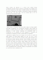
Figure 7: Typical parallel-plate reactive ion etching system.
3. Appartus & Reagents
1) Appratus : Spin coater, UV exposure, Tester coil, Heat palter, Glass
2) Reagents : DEVELOPER-AZ400K, PDMS(Polydimethylsiloxane), PR-AZ1512
4. Procedure
1) Cleaning Process
First, you immerse the glass in DeIonized Water(minimum 10minute). And then, you clean the glass in order of Acetone, IPA and DeIonized Water and purge with N2 gas. At this time, you must put the glass in petri-dish quickly after cleaning.
2) Lithography Process
After cleaning process, you have to do lithography process. Purpose of lithography is pattering on wafer. This is process of lithography. First, you dope PR(photoresist) on wafer(cleanin glass). In this step, you run following 3 steps of spin coating by using PR-AZ1512. You run spin coater in RPM 2000, 5sec, and RPM 1000, 40sec, and RPM 2000, 5sec. And then, you do soft baking process. Soft baking process is done on heat plate at 120℃, 90sec. In third step, you do photo process. Photo process is putting the mask(printing your name on transparent paper like OHP film to make mask) on the glass and exposure UV in vacuum condition for 300sec. After Photo process, you put the glass inside developer-AZ400K for development. This step is 'Develop process'. Finally, you do hard baking on heat plate at 120℃, 90sec.
3) Assembling process
First, you mix the PDMS with PDMS curing agent with a ratio of 10:1 and cast on developed glass. Second, you peel off the cured(crosslinked) PDMS from the glass. Finally, treat the surface of PDMS with tesler coil and put it on surface of glass.
Vapor phase etching is another dry etching method, which can be done with simpler equipment than what RIE requires. In this process the wafer to be etched is placed inside a chamber, in which one or more gases are introduced. The material to be etched is dissolved at the surface in a chemical reaction with the gas molecules. The two most common vapor phase etching technologies are silicon dioxide etching using hydrogen fluoride (HF) and silicon etching using xenon diflouride (XeF2), both of which are isotropic in nature. Usually, care must be taken in the design of a vapor phase process to not have bi-products form in the chemical reaction that condense on the surface and interfere with the etching process.
- When do I want to use dry etching?
The first thing you should note about this technology is that it is expensive to run compared to wet etching. If you are concerned with feature resolution in thin film structures or you need vertical sidewalls for deep etchings in the substrate, you have to consider dry etching. If you are concerned about the price of your process and device, you may want to minimize the use of dry etching. The IC industry has long since adopted dry etching to achieve small features, but in many cases feature size is not as critical in MEMS. Dry etching is an enabling technology, which comes at a sometimes high cost.
Figure 7: Typical parallel-plate reactive ion etching system.
3. Appartus & Reagents
1) Appratus : Spin coater, UV exposure, Tester coil, Heat palter, Glass
2) Reagents : DEVELOPER-AZ400K, PDMS(Polydimethylsiloxane), PR-AZ1512
4. Procedure
1) Cleaning Process
First, you immerse the glass in DeIonized Water(minimum 10minute). And then, you clean the glass in order of Acetone, IPA and DeIonized Water and purge with N2 gas. At this time, you must put the glass in petri-dish quickly after cleaning.
2) Lithography Process
After cleaning process, you have to do lithography process. Purpose of lithography is pattering on wafer. This is process of lithography. First, you dope PR(photoresist) on wafer(cleanin glass). In this step, you run following 3 steps of spin coating by using PR-AZ1512. You run spin coater in RPM 2000, 5sec, and RPM 1000, 40sec, and RPM 2000, 5sec. And then, you do soft baking process. Soft baking process is done on heat plate at 120℃, 90sec. In third step, you do photo process. Photo process is putting the mask(printing your name on transparent paper like OHP film to make mask) on the glass and exposure UV in vacuum condition for 300sec. After Photo process, you put the glass inside developer-AZ400K for development. This step is 'Develop process'. Finally, you do hard baking on heat plate at 120℃, 90sec.
3) Assembling process
First, you mix the PDMS with PDMS curing agent with a ratio of 10:1 and cast on developed glass. Second, you peel off the cured(crosslinked) PDMS from the glass. Finally, treat the surface of PDMS with tesler coil and put it on surface of glass.
추천자료
 [화공기초실험] 비중 및 밀도 측정(예비레포트)
- [화공기초실험] 어는점 내림법에 의한 분자량 측정(예비레포트)
- [화공기초실험] 어는점 내림법에 의한 분자량 측정(결과레포트)
- [화공기초실험] 산화 환원 적정(예비레포트)
- [화공기초실험] 산화 환원 적정(결과레포트)
- [화공기초실험] 재결정(예비레포트)
- [화공기초실험] 재결정(결과레포트)
- [화공기초실험] pH 측정(결과레포트)
- 화공실험 건조
- [화공실험] 이중관 열교환기 : 이중관의 열교환장를 사용하여 난류상태에서 열전달 특성 이해...
- [화공실험] 하이시스(HYSYS) 이용한 공정 시뮬레이션 SIMULATION 결과 : n-Heptane 추출하고 ...
- [화공실험] 유체마찰 손실 및 유량측정 결과 : 교축유량계의 작동 및 측정원리, 유량 측정 숙...
- [화공실험] 오렌지Ⅱ의 합성 (디아조화 반응과 커플링 반응) 결과 : 술파닐산을 디아조화하고,...
- [화공실험] CO2 흡수 : 물에 의한 CO2의 흡수실험을 통하여 물질전달 이론을 이해하고 액체를...
- 가격2,000원
- 페이지수14페이지
- 등록일2011.03.05
- 저작시기2010.9
- 파일형식한글(hwp)
- 자료번호#653936

본 자료는 최근 2주간 다운받은 회원이 없습니다.