


-
1
-
2
-
3
-
4
-
5
-
6
-
7
해당 자료는 2페이지 까지만 미리보기를 제공합니다.
2페이지 이후부터 다운로드 후 확인할 수 있습니다.
2페이지 이후부터 다운로드 후 확인할 수 있습니다.


목차
■ Abstract ..............................................page. 1
■ Introduction ..................................page. 1
■ Phase Change Memory ............................page. 1
1. About the Phase Change Memory ........................page. 1
1-1. Operation Theory of the Phase Change Memory .......page. 2
1-2. The most promising Memory - PRAM ..................page. 3
2. The features of the Phase Change Memory ..............page. 3
2-1. The advantages of the Phase Change Memory .........page. 4
2-2. The disadvantages of the Phase Change Memory ............page. 4
3. The Development of the Phase Change Memory ..........page. 5
■ Conclusions ..................................page.6
■ References .......................................page.7
▣ FIGURE CONTENTS ▣
< Figure 1. Set-reset principle of PRAM device based GST and Basic structure. >
< Figure 2. Electrical switching of PC materials for non-volatile electronic storage >
< Figure 3. Calculated electron densities in arbitrary units >
----------------▣
▣ TABLE CONTENTS ▣
< Table 1. Feature of PRAM comparing other novel promising memories >-------▣
본문내용
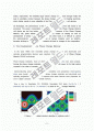
Now a day, In Rewritable CD, DVDRAM, Rewritable DVD disks Ge-Sb-Te ( 3 elements) and Ag-In-Sb-Te ( 4 elements ) is used as Phase Change Materials.
< Figure 3. Calculated electron densities in arbitrary units >
Ge-Sb-Te ( 3 elements) is used in PD, DVD-RAM, DVD-RW. And Ag-In-Sb-Te( 4 elements ) is used in CD-RW, DVD-RW. Current technology makes CD-RW possible to write / rewrite almost 1,000time, in case of DVD-RAM almost 500,000 time.
In 2002 International Solid-State Circuits Conferences(ISSCC) Intel Corp., Ovonyx Corp., Azalea Corp, three companies reported PRAM device using GexSbyTez. That was first time of PRAM technology application. That chip name is Ovonic Unified Memory(OUM) ,made by 0.18㎛ CMOS process , and demonstrate possibility to combination PRAM with CMOS process
Ovonyx Corp. AFRL. BAE systems make by using radiation-hardened CMOS process PRAM device based Chalcogenide. Chalcogenide was composed 1Transistor-1Resistor system.
The phase change materials is the most important substance in optical memory. In CD-ROM, DVD, DVD-RAM many studies have been reported. Ge2Sb2Te5 is very well known for its high optical contrast in the state of amorphous and crystalline. However, the characteristics required in solid state memory are quite different from optical ones. The structural properties of GeSbTe thin films with composition is investigated for PRAM.
ETRI 및 연세대 등에서는 PRAM 소자 개발에 신규 재료인 안티몬(Sb)과 셀라늄(Se)이 혼합된 이원계 금속 합금인 Sb-Se 상변화 재료를 사용하여 GTS에 비해 재료의 녹는점이 낮고 결정화에 필요한 시간이
추천자료
 기술중심 시대의 전망, 기업의 기술경영과 R&D 방향성
- 디지털기술과 인간의 행복
- 현대기술의 역사와 기술 변화의 쟁점
- 기술과 사회 정리
- 사과의 결점판정 선별시스템 개발을 위한 영상처리프로그램 및 알고리즘 개발
- [섬유][섬유제품][섬유가공][섬유제품가공기술][섬유기술]섬유의 정의, 섬유의 종류, 섬유의 ...
- [나노기술][나노][NANO][탄소나노튜브]나노기술(나노, NANO)의 개념과 나노기술(나노, NANO)...
- 초등학교 정보통신기술(ICT)활용교육의 운영 방향, 초등학교 국어과와 영어과의 정보통신기술...
 기술 경영
기술 경영- [초전도체][초전도체 정의][초전도체 특성][초전도체와 전기전도][초전도체 성형법][초전도체...
- [정보관리][노숙자 정보관리][정보자원관리][정보기술관리][개인정보관리][저작권정보관리]저...
- [웅진식품][웅진식품 역사][웅진식품 개발철학][웅진식품 기업정신][웅진식품 기업이념]웅진...
- [무선통신 반도체][무선통신 반도체 유비쿼터스][무선통신 반도체 신소자 기술]무선통신 반도...
- 가격1,200원
- 페이지수7페이지
- 등록일2010.01.13
- 저작시기2009.6
- 파일형식한글(hwp)
- 자료번호#573998

본 자료는 최근 2주간 다운받은 회원이 없습니다.


소개글